Fast electron imaging of biological specimens using multibeam scanning electron microscopy
- Abstract number
- 218
- Event
- European Microscopy Congress 2020
- DOI
- 10.22443/rms.emc2020.218
- Corresponding Email
- [email protected]
- Session
- LST.4 - Volume Scanning Electron Microscopy in life sciences
- Authors
- Dr. Job Fermie (2), Wilco Zuidema (1, 2), Radim Šejnoha (3), Dr. Jacob Hoogenboom (1), Prof. Dr. Pieter Kruit (1)
- Affiliations
-
1. Delft University of Technology
2. Delmic
3. Thermo Fisher Scientific
- Keywords
electron microscopy, multibeam, multibeam electron microscopy, STEM, volume EM
- Abstract text
Electron microscopy (EM) is increasingly being used in large-scale biological projects, either for volume imaging or large area mapping. In both use cases, a need for increased throughput, reliability and automation of electron microscopy highlights the importance for a new approach to large-scale imaging. Here, we demonstrate the working principles and image collection in a streamlined multibeam STEM system based on the prototypes developed in collaboration between Delmic, TU Delft, Thermo Fisher Scientific and Technolution.
With the increasing need for large-volume ultrastructural data, and large numbers of samples, a high sustained imaging throughput becomes paramount. Conventional electron microscopy (EM) however is incapable of increasing imaging speed without sacrificing image quality. To overcome this challenge, we have developed an automated multibeam scanning EM which combines simultaneous 64-beam electron imaging with sensitive transmission electron detection (optical STEM, OSTEM). By increasing imaging speed and reducing operator overhead, this imaging approach presents a substantial improvement for high-throughput EM of biological specimens.
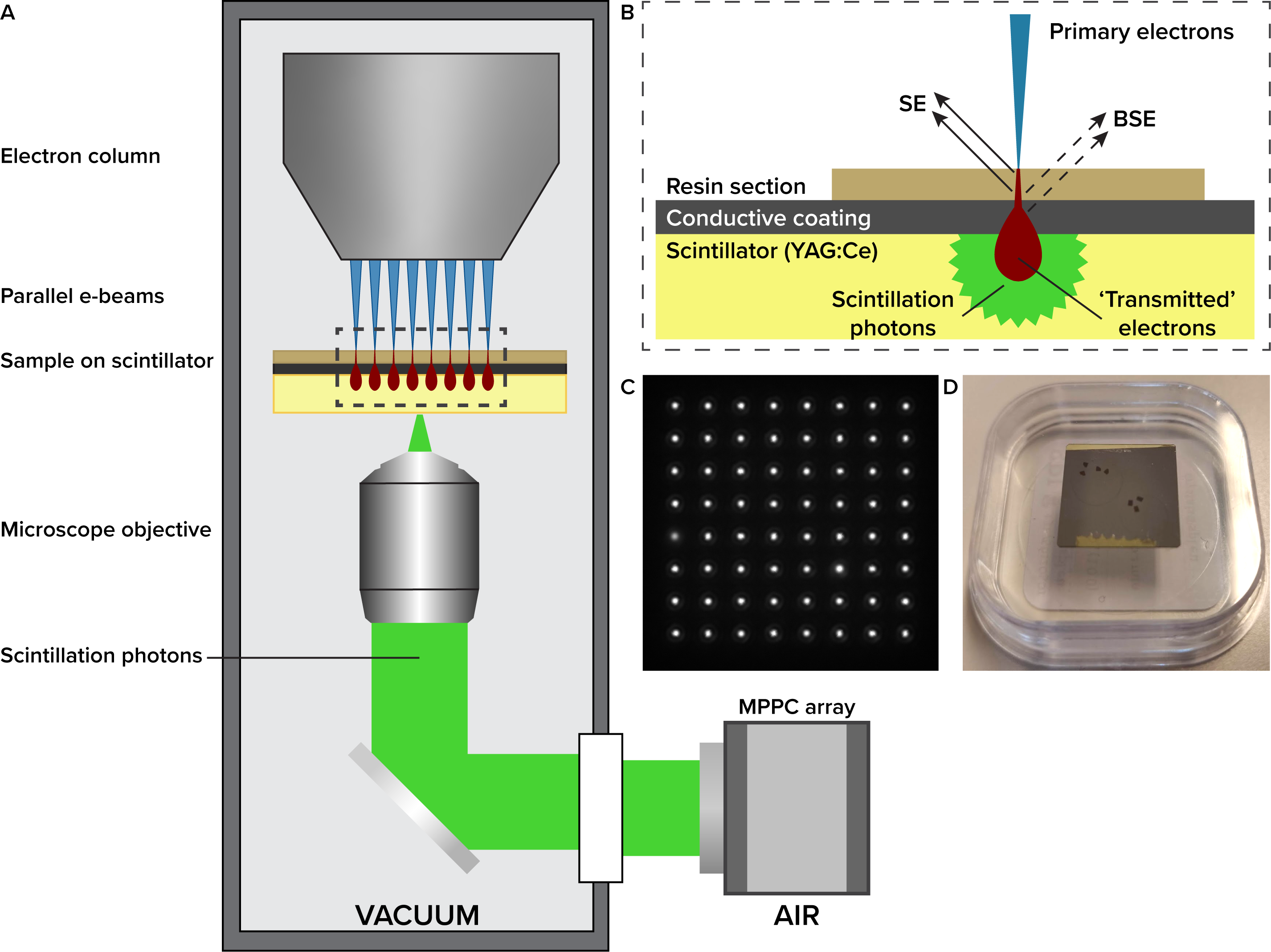
We developed multibeam electron optics that produce an 8*8 square array of electron beamlets with a current of 200 pA per beamlet, which are focused on the sample in one plane (figure 1A). The 64 beamlets are scanned over the sample simultaneously, so that every beamlet scans an area of 3.2*3.2 μm. Thus, one scan covers a field of 25.6*25.6 μm. Electron detection is achieved through an optical detection pathway, where electrons transmitted through a sample produce light in a scintillator substrate (figure 1B, C) [1,2]. Since light intensity depends on the number and energy of electrons hitting the scintillator plate, fluctuations in the light intensity are a metric for the electron density of the sample. As a detector, a rapid multi-pixel photon counter array is used, enabling fast scan rates with a pixel dwell time of 250 ns.
Figure 1 Working principles of the multibeam EM. (A) Schematic of the multibeam electron microscope. (B) Sample geometry for the multibeam. Electrons transmitted through the sample produce photons in the scintillator, which are detected on the MPPC array. (C) Image of 64 scintillating spots in the scintillator, captured on a CMOS camera. To form a gray-scale micrograph, the intensity variation of individual spots is recorded with the MPPC array as the beams scan over a sample. (D) Photograph of 80 nm epon sections deposited on scintillator substrate.
The quality of the final multibeam image is determined by the uniformity of beamlets in terms of resolution and current. Using the system presented here, we aimed to validate the quality of image formation, by testing the quality of individual beamlets in the multiprobe.
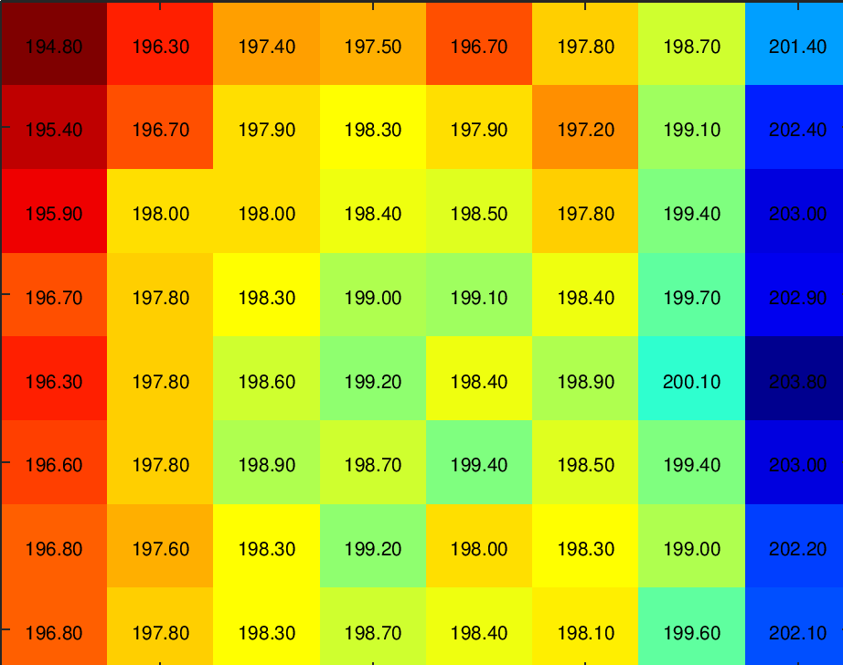
Variations in beamlet current will result in image quality differences between individual image tiles, mainly contrast and signal-to-noise ratio. A measurement on the system was performed in order to ensure beamlet current uniformity, the result is shown in figure 2. The average beamlet current was found to be 198.6 pA with a standard deviation of 1.9 pA.
Figure 2 Heatmap showing the current of the 64 individual beamlets of the tested system. Minimal current deviations are seen over the array of beams.
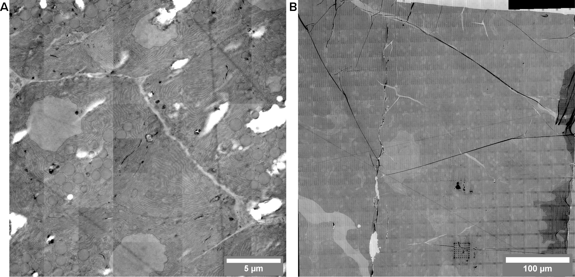
After validation of the beamlet quality, we further developed our system for large-scale imaging. Using the transmission detector high quality field images can be acquired of biological material (figure 3A). With stage movement routines, these fields can be rapidly tiled to form ‘megafields’, comprising of many multibeam fields. Such a megafield is shown in figure 3B, where we demonstrate the potential of the multibeam system for large-scale acquisition by capturing a 16.4 gigapixel megafield in 45 minutes. Such a dataset would take a minimum of 3 hours and 40 minutes in a singlebeam SEM at similar dwell time settings. While this result is not yet a 64-fold increase in throughput, it should be noted that this single-beam estimate does not account for overhead like focusing and stage movement. Steps like these can rapidly increase the total required project time by over 30-40% [3]. In addition, ongoing development of a new, faster stage hardware and streamlining of the acquisition pipeline will enable further increases in sustained throughput.
Figure 3 Single field (A) and megafield (B) of rat pancreas acquired in 64 beam multibeam STEM. (A) Single image showing the 8*8 pattern used to build up a single field. Seamless stitching of the 64 sub images is consistently achieved. Images were acquired at 5kV landing energy, 4 nm pixel size, 3200 ns dwell time. (B) 20*20 megafield. Raw pixel count is 128000*128000 pixels (16.4 gigapixels), acquired in 45 minutes. Images were acquired at 5kV landing energy, 4 nm pixel size and 800 ns dwell time. Final field of view after stitching 435*435 μm. Singlebeam equivalent without accounting overhead: 3h40m. Samples courtesy of Ben Giepmans.
In conclusion, continued development of the multibeam electron microscope in Delft has resulted in a 64-beam SEM equipped with rapid transmitted electron detector. Multibeam electron imaging combined with optical STEM detection provides a significant improvement in imaging throughput over conventional single-beam systems, without compromising on image contrast or morphological detail in biological material. High-throughput imaging systems like the one described here will be instrumental in tackling increasingly common large-scale imaging projects, by offering nanometer resolution over millimeter-scale fields of view.
- References
[1] A. Mohammadi-Gheidari et al. Journal of Vacuum Science & Technology B 28 (2010), pC6G5-C6G10
[2] Y. Ren and P. Kruit. Journal of Vacuum Science & Technology B 34 (2016), p06KF02-01-06KF02-10
[3] B. Titze, and C. Genoud. Biology of the Cell, 108(11) (2016), p307–323.