High Resolution S/TEM Study of Vertical and In-Plane Heterostructures Formed by Two-Dimensional MoS2 and ReS2
- Abstract number
- 1283
- Event
- European Microscopy Congress 2020
- DOI
- 10.22443/rms.emc2020.1283
- Corresponding Email
- [email protected]
- Session
- PSA.1 - 1D & 2D Materials
- Authors
- Mr. Saiphaneendra Bachu (1), Ms. Lauren Stanton (1), Mr. Chenhao Qian (1), Dr. Danielle Reifsnyder Hickey (1), Dr. Nasim Alem (1)
- Affiliations
-
1. Pennsylvania State University
- Keywords
Anisotropy, Epitaxy, HAADF-STEM, Heterostructures, Two-dimensional (2D) materials
- Abstract text
Low dimensional (zero, one and two dimensional) materials attracted great attention from researchers owing to their novel properties arising from quantum confinement and surface/interface effects [1]. Two-dimensional (2D) transition metal dichalcogenides (TMD), such as MoS2 and WSe2, are particularly interesting because of their semiconductor nature and transition from indirect to direct band gap when thinned down to a single layer [2]. This opened up a lot of opportunities in band structure engineering towards applications in optoelectronics. One such example of band structure engineering is integrating multiple 2D TMD into heterostructures in vertical and in-plane geometries. For example, C. Zhang et al. observed that the lattice mismatch strain at the interface of MoS2-WSe2 in-plane heterostructures is relieved by forming dislocations at the interface and that changes the band alignment from type II to type I [3]. This means the performance of the heterostructures towards targeted applications is highly dependent on careful selection of constituent TMD and the interfaces formed between them.
This study explores vertical and in-plane heterostructures formed by MoS2 and ReS2. MoS2-ReS2 heterostructures are a fascinating material system to study because MoS2 is isotropic in nature whereas ReS2 has an anisotropic structure thus forming isotropic-anisotropic interface [4]. Such anisotropy in the system could introduce modulations in the atomic and interfacial structure and lead to polarization dependent optical properties [5]. Therefore, it is important to understand the atomic structure of the MoS2-ReS2 interface before this material system could be incorporated into any applications.
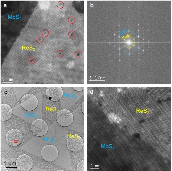
This work covers synthesis and atomic scale structural characterization of vertical and in-plane MoS2-ReS2 heterostructures. Synthesis of the heterostructures was carried out using a two-step powder-source chemical vapor deposition (CVD) process on sapphire substrates [6]. The as-grown heterostructures were characterized using aberration-corrected high-angle annual dark-field (HAADF) scanning transmission electron microscopy (STEM) to understand interface atomic structure and, epitaxy and strain between the MoS2 and ReS2 layers. An FEI Titan3 G2 operated at 80 kV was employed to perform HAADF-STEM imaging. Atomic resolution HAADF-STEM image of a vertical heterostructure showing the underlying monolayer MoS2 with monolayer ReS2 crystal grown on top is presented in Figure 1a. A closer look at the image reveals the Re chains in ReS2 align with the zigzag direction of MoS2 which means ReS2 grows epitaxially on top of MoS2. This is also confirmed by the matching orientation of FFT spots of MoS2 and ReS2 in Figure 1b. Dashed red circles in Figure 1a indicate vacancy clusters present in the ReS2 lattice highlighting the defective nature of ReS2 layer grown during synthesis. Figure 1c is a low magnification TEM image showing in-plane heterostructures of MoS2 and ReS2, wherein ReS2 grows in the gap between MoS2 triangles during the second step of the synthesis procedure. An atomic resolution HAADF-STEM image taken from the edge of a MoS2 triangle, as outlined by a red box in Figure 1c, is shown in Figure 1d. The presentation will further dwell into quantitative analysis of various features seen in the heterostructures [7].
Figure 1 MoS2-ReS2 vertical heterostructures: (a) atomic resolution HAADF-STEM image of vertical heterostructure showing monolayer ReS2 grown on top of monolayer MoS2 and (b) binned FFT pattern obtained from (a) highlighting the epitaxy between MoS2 an ReS2; MoS2-ReS2 in-plane heterostructures: (c) Low-magnification TEM image showing MoS2 triangles with ReS2 grown between the triangles and (d) atomic-resolution HAADF-STEM image of in-plane heterostructure formed at the edge of a MoS2 triangle, obtained from the region marked by the red box in (c).
- References
[1] Pakdel, Amir, et al. Materials Today 15.6 (2012): 256-265.
[2] Jariwala, Deep, et al. ACS nano 8.2 (2014): 1102-1120.
[3] Zhang, Chendong, et al. Nature Nanotechnology 13 (2018): 152–158.
[4] Lin, Yung-Chang, et al. ACS Nano 9.11 (2015): 11249-11257.
[5] Neupane, Guru Prakash, et al. Small 15 (2019): 1804733.
[6] Chen, Bin, et al. Advanced Materials 29.34 (2017): 1701201.
[7] This work was supported by the National Science Foundation (NSF), in part under the CAREER program (DMR-1654107), in part by the program EFRI 2-DARE: 2D Crystals by Activated Atomic Layer Deposition (EFRI-1433378), and in part by the Penn State 2D Crystal Consortium-Materials Innovation Platform (2DCC-MIP) under NSF cooperative agreement DMR-1539916.

