Machine learning for high-resolution transmission electron microscopy images defect recognition
- Abstract number
- 1371
- Event
- European Microscopy Congress 2020
- DOI
- 10.22443/rms.emc2020.1371
- Corresponding Email
- [email protected]
- Session
- DHA.1 - Deep learning for analysis and interpretation of microscopy imaging data
- Authors
- Mr Nik Dennler (2), Dr Antonio Foncubierta Rodriguez (1), Ms Marilyne Sousa (1)
- Affiliations
-
1. IBM Research GmbH
2. University of Zurich, Institute of Neuroinformatics
- Keywords
HRTEM, Machine Learning, Defect recognition
- Abstract text
We investigate the detection and segmentation of crystalline lattice defects in novel materials and devices from High-Resolution Transmission Electron Microscopy (HRTEM) images. We make use of different methods of computer vision and machine learning for building a system that assists materials characterization experts in performing efficient and robust analyses.
In recent years, tremendous progresses have been made in the field of machine learning for large data set analyses in material sciences1. However, scientists do not always have enough data to create a reliable algorithm; this is particularly true in the field of transmission electron microscopy, where obtaining images is time consuming. Namely, a sample must first be prepared, and then the microscopist typically acquires only a few relevant images for the purpose of his/her study, which images are usually pretty large. The process can become quite complex when looking for crystalline defects in HRTEM images, as such defects cause a break in the material lattice periodicity, which only impacts a tiny portion of the images.
This work aims at identifying defects on HRTEM images acquired on III-V materials deposited in-house by metalorganic chemical vapor deposition (MOCVD) on silicon substrates. Due to their high mobility and direct band gap, III-V materials are regarded as very promising materials for obtaining novel, high-performance devices for electronic and photonic applications. However, the lattice mismatch between the silicon and the III-V often leads to crystalline defects that impact the devices performance. It is accordingly crucial for material scientists to track such defects in a robust and reliable manner.
Our approach elaborates on different combinations of algorithms, which could be useful in providing HRTEM users with an assistant in the defect detection process. The tested algorithms cover various techniques of both traditional and modern computer vision; including different pre-processing steps, using local and patch-wise Fourier transformations, handcrafted and automatically generated convolutional image filters and classifying image patches with machine learning approaches, such as principal component analysis, convolutional neural networks and anomaly-detecting variational autoencoders. We find that for many algorithms, while they perform well for the application presented in literature, they do not yield satisfactory results on our data sets. Indeed, they are not suitable due to constraints of the imaging technique and data availability, or they simply lack generality. Therefore, we developed an original method that combines some of the above techniques in an unique way, and satisfactorily performs on our data set. Tested against different evaluation metrics and human expert opinions, we believe that our system is well suited for assisting both HRTEM experts and casual users in tedious analyses.
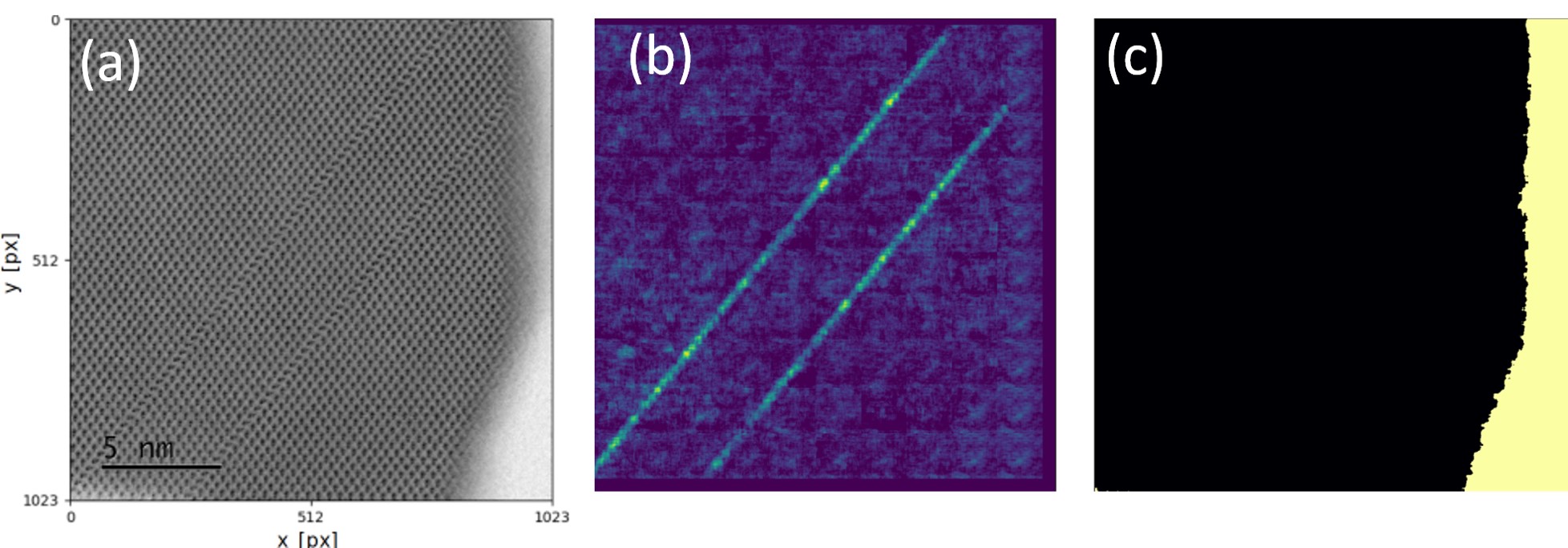
(a) HRTEM image of a defective III-V material: after filtering, we could highlight the lattice defects (b) as well as discriminate the amorphous from the crystalline area (c)
The authors thank S. Mauthe, Y. Baumgartner and H. Schmid for their technical support, P. Staudinger for providing HRTEM images and Prof. Dr. T. Neupert from the University of Zurich (Switzerland) for fruitful discussions.
Financial support from the EU DESIGN EID (860095) project is also acknowledged.- References
1 J. Schmidt et al. “Recent advances and applications of machine learning in solid state materials science”, npj Computational Materials, 5:83, 2019

