Photoluminescence Yield Enhancement at Atomically-Thin Flake Edges of WSe2
- Abstract number
- 1432
- Event
- European Microscopy Congress 2020
- DOI
- 10.22443/rms.emc2020.1432
- Corresponding Email
- [email protected]
- Session
- PSA.1 - 1D & 2D Materials
- Authors
- Dr. Steffi Woo (2), Johann Preuß (1), Robert Schneider (1), Dr. Steffen Michaelis de Vasconcellos (1), Prof. Rudolf Bratschitsch (1), Dr. Luiz Tizei (2)
- Affiliations
-
1. Institute of Physics and Center for Nanotechnology, University of Münster
2. Laboratoire de Physique des Solides, Université Paris-Saclay, CNRS
- Keywords
2D materials, electron energy-loss spectroscopy, photoluminescence, single photon emitters, transition metal dichalcogenides
- Abstract text
Single- and few-layer semiconducting transition metal dichalcogenides (TMDCs) demonstrate to be a fascinating class of two-dimensional (2D) materials that can act as building blocks for van der Waals heterostructures. Standalone, bulk and multi-layered tungsten diselenide (WSe2) are indirect gap semiconductors, while its monolayers exhibit a direct optical bandgap in the visible. At cryogenic temperature, the photoluminescence (PL) response of monolayer WSe2 is typically composed of the neutral A exciton (X0), charged exciton (trion, X– or X+) emission, and a dominant broad defect-bound exciton band [1]. Recently, bright and stable single-photon emitters from localized excitons in WSe2 monolayers overlapping the broad defect band have been demonstrated [2–4], with tendencies to appear at monolayer and few-layer edges [2,3]. This feature was further exploited to deliberately create centers at generated folded edges within WSe2 monolayers using a micron-sized metal tip [3].
The nature of such single-photon emitters remains highly debated, with speculations suggesting nanometer-sized monolayer fragments [2,5] or curling at flake edges [2], structural defects or inhomogeneous strain [3,6]. A gap in the understanding encourages correlation of the optical response to the origin of the single-photon emitters. It is thus critical to understand the structural variation at the scale of atomic defects, such as isolated anion vacancies, through to the nanometric scale with local strain and bending of atomically-thin TMDC layers. Aberration-corrected and monochromated scanning transmission electron microscopy (STEM) is the platform capable of bridging the nanometric optical response to the atomic-scale structural properties.
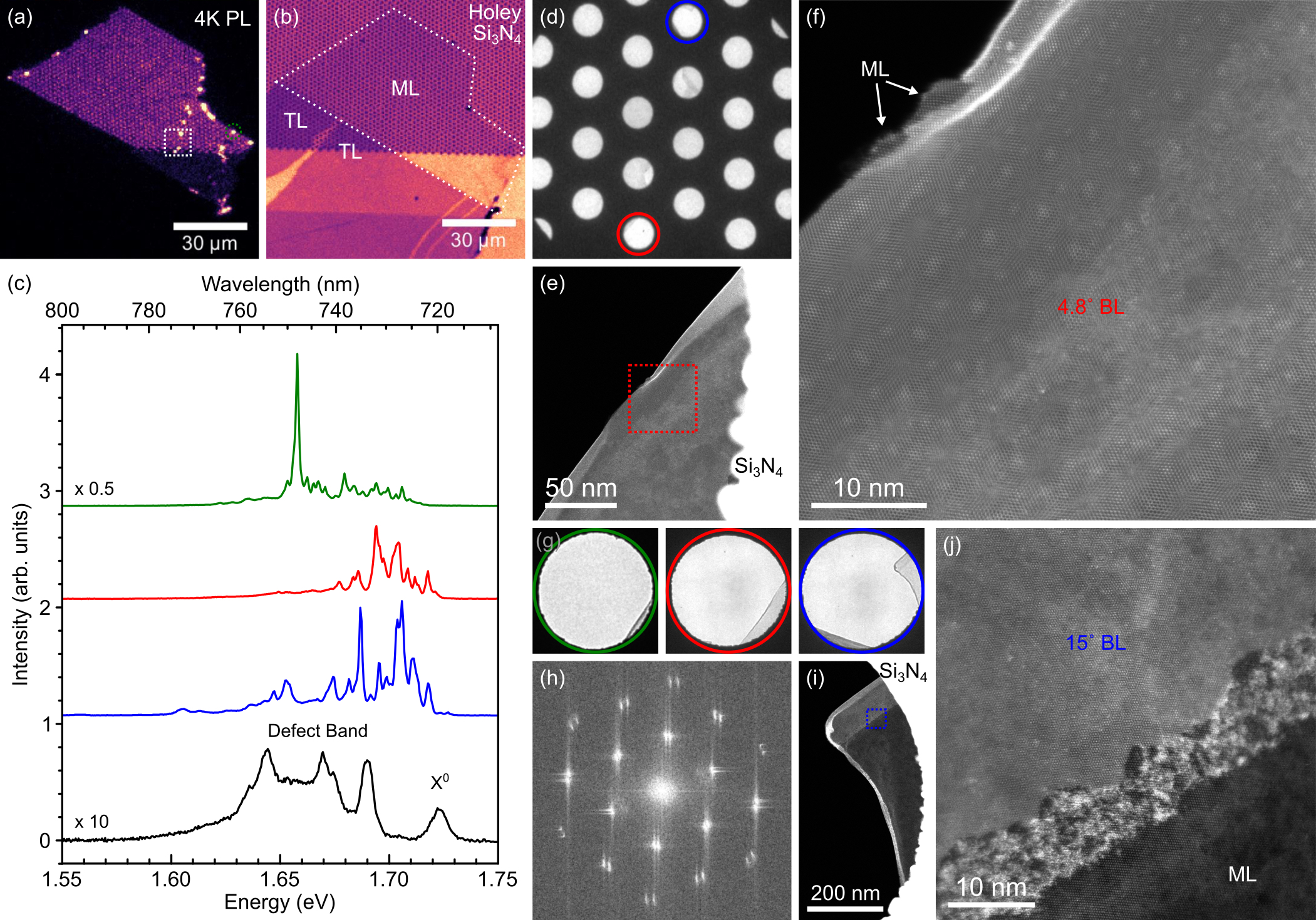
Atomically-thin WSe2 flakes have been mechanically exfoliated from a bulk synthetically-grown crystal, and transferred onto a Si3N4 TEM grid with periodic micron-sized holes. Spatially-resolved PL of the freestanding WSe2 is excited with a continuous wave 532 nm laser using a scanning confocal setup equipped with a helium cryostat (T = 4 K). Atomically-resolved imaging has been performed on a Nion UltraSTEM200 operated at 60 keV and monochromated electron energy-loss spectroscopy (EELS) on a modified Nion HERMES-S200 (ChromaTEM) operated at 60 kV at liquid nitrogen temperatures (T ≈ 100 K). 4K-PL identifies multiple localized emission lines overlapping the broad defect band in each of the holes containing a freestanding WSe2 monolayer, with some holes exhibiting narrow lines in the order of 100s µeV [Fig. 1(c)]. Moreover, the 4K-PL micrograph in Fig. 1(a) shows hot spots along flake edges where there is an increase in PL intensity of these narrow lines compared to their inner part. Subsequent high-angle annular dark-field (HAADF) imaging in STEM of these areas confirms that the majority of the hot spots contain only partial coverage of WSe2 within the hole instead of the continuous monolayer (ML) expected, including folded MLs with non-zero twist angle, and scroll/tubes at freestanding flake edges [Fig. 1(d–i)]. In addition, regions with (twisted) bilayers (BL) are present. The excitonic signatures of these structurally-unique features at the nanoscale is also explored using monochromated STEM-EELS [7].
Fig. 1: (a) Photoluminescence (PL) intensity map of the region shown in the optical reflection micrograph in (b). (c) PL spectra from selected holes marked in the same color code as the PL map (a) the low-magnification STEM bright-field (BF) image in (d). STEM-HAADF images of the WSe2 layers from the holes marked in red (e,f) and blue (i,j) from the BF image in (g, flipped horizontally and 90˚ clockwise rotated relative to (d)), detailing in (f) a folded ML resulting in a BL with 4.8˚ twist angle measured from the image fast-Fourier transform in (h) and a 100 nm wide fragment of 15˚ twisted BL in (j).
- References
[1] Jones, A.M., Yu, H., Ghimire, N. et al. Optical generation of excitonic valley coherence in monolayer WSe2. Nature Nanotech. 8, 896–869 (2013).
[2] Koperski, M., Nogajewski, K., Arora, A. et al. Single photon emitters in exfoliated WSe2 structures. Nature Nanotech. 10, 503–506 (2015).
[3] Tonndorf, P., Schmidt, R., Schneider, R., Kern, J., Buscema, M., Steele, G.A., Castellanos-Gomez, A., van der Zant, H.S.J., Michaelis de Vasconcellos, S. and Bratschitsch, R. Optica 2, 347 (2015).
[4] He, Y., Clark, G., Schaibley, J. et al. Single quantum emitters in monolayer semiconductors. Nature Nanotech. 10, 497–502 (2015).
[5] Srivastava, A., Sidler, M., Allain, A. et al. Optically active quantum dots in monolayer WSe2. Nature Nanotech. 10, 491–496 (2015).
[6] Kern, J., Niehues, I., Tonndorf, P. et al. Nanoscale positioning of single-photon emitters in atomically thin WSe2, Adv. Mat. 18, 7401 (2016).
[7] The authors acknowledge funding from the ANR, program of future investment TEMPOS-CHROMATEM (No. ANR-10-EQPX- 50), and the European Union in the Horizon 2020 Framework Program (H2020-EU) under Grant Agreement No. 823717 (ESTEEM3).

