Photonic Chip-assisted Correlative Light and Electron Microscopy
- Abstract number
- 1413
- Event
- European Microscopy Congress 2020
- DOI
- 10.22443/rms.emc2020.1413
- Corresponding Email
- [email protected]
- Session
- LST.5 - Correlative Microscopy across the scales
- Authors
- Jean-Claude Tinguely (3), Anna Steyer (2, 1), Cristina Ionica Øie (3), Øystein Helle (3), Firehun Tsige Dullo (3), Randi Olsen (3), Peter McCourt (3), Yannick Schwab (1), Balpreet Singh Ahluwalia (3)
- Affiliations
-
1. European Molecular Biology Laboratory
2. Max Planck Institute of Experimental Medicine
3. UiT The Arctic University of Norway
- Keywords
CLEM, Integrated Optics, LSECs, super-resolution optical microscopy, waveguides
- Abstract text
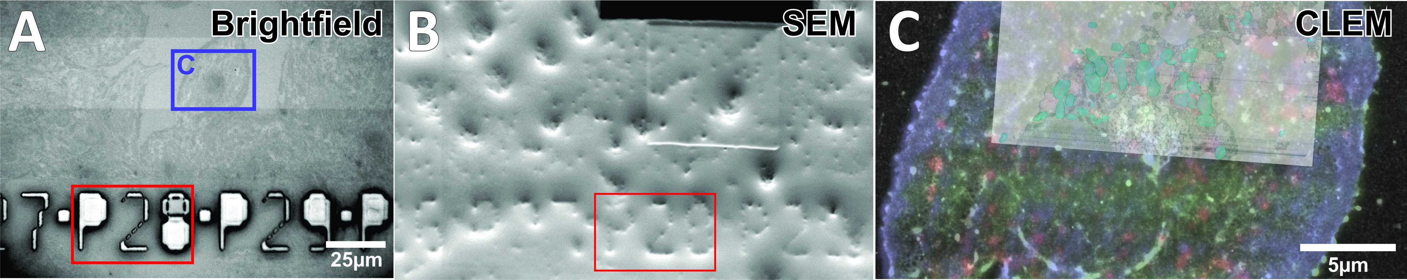
Correlative light-electron microscopy (CLEM) unifies the versatility of light microscopy (LM) with the high resolution of electron microscopy (EM), allowing one to zoom into the complex organization of cells. Most CLEM techniques use ultrathin sections, and thus lack the 3D-EM structural information, focusing on a very restricted field of view. Photonic chip-based imaging has been introduced as a multi-modal bioimaging platform for total internal reflection fluorescence (TIRF), offering unprecedented large field of view, easy wavelength multiplexing [1], and on-chip implementation of different super-resolution methodologies [2, 3]. Here, we present photonic chip-assisted CLEM, providing the photonic chip advantages together with high precision localization of the target area of interest within EM. The chip-based direct stochastic optical reconstruction microscopy (dSTORM), and 3D high precision correlation of biological processes by focused ion beam-scanning electron microscopy (FIB-SEM) is further demonstrated (Figure 1). The photonic chips are used as substrate and illumination source, enabling high-precision landmarking of the sample through specially designed grid-like numbering systems. The landmarks are fabricated on the cladding of the photonic chips as extruding pillars from the waveguide surface, thus remaining visible for FIB-SEM after resin embedding during sample processing. Using this approach we demonstrate its applicability for tracking the area of interest, imaging the 3D structural organization of nano-sized morphological features on liver sinusoidal endothelial cells such as fenestrations, and correlating specific endo-lysosomal compartments with its cargo protein upon endocytosis. We envisage that photonic chip equipped with landmarks can be used in the future to automatize the work-flow for both LM and EM for high-throughput CLEM, providing the resolution needed for insights into the complex intracellular communication and the relation between morphology and function in health and disease.
Figure 1: A) Brightfield image of liver sinusoidal endothelial cells seeded on photonic chip. B) Resin-embedded chip under SEM, with visible landmarks. C) Correlated 3-color TIRF, dSTORM and EM imaging, with 3D reconstruction of lysosomes in light blue.
- References
[1] J-C. Tinguely, Ø.I. Helle, and B.S. Ahluwalia. “Silicon nitride waveguide platform for fluorescence microscopy of living cells”, Optics Express 25 (2017), 27678-27690.
[2] R. Diekmann, Ø.I. Helle, C.I. Øie, P.A. McCourt, T.R. Huser, M. Schüttpelz, and B.S. Ahluwalia. “Chip-based wide field-of-view nanoscopy”, Nature Photonics 11 (2017), 322-328.
[3] Ø.I. Helle, F.T. Dullo, M. Lahrberg, J.-C. Tinguely, and B.S. Ahluwalia. “Structured illumination microscopy using a photonic chip”, Nature Photonics, accepted for publication (2020).